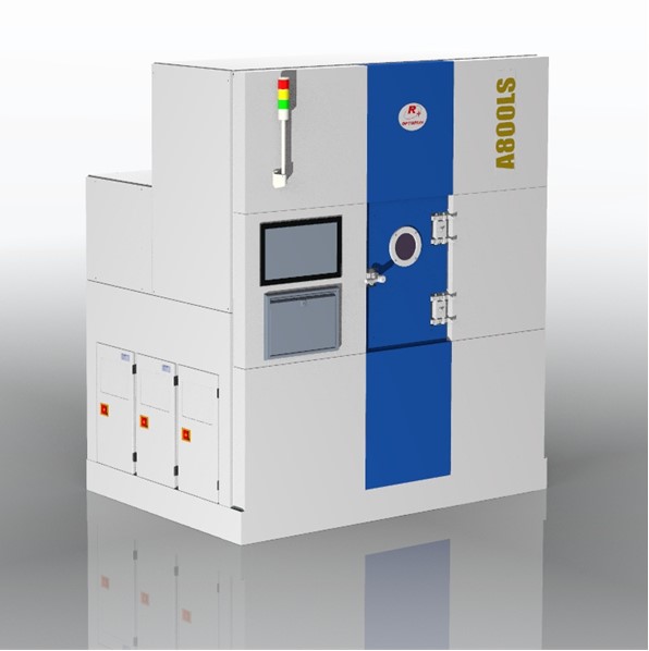
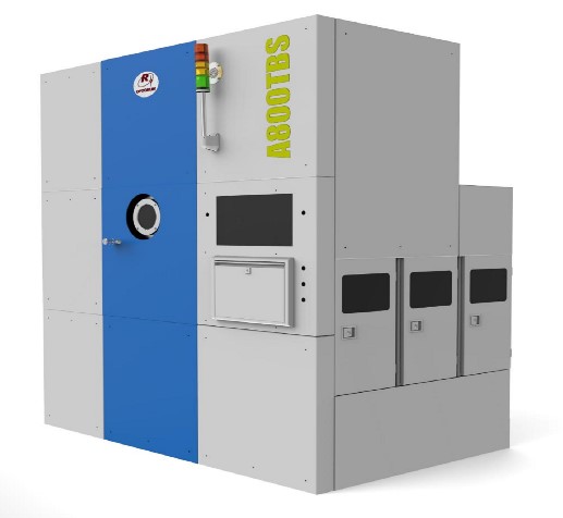
Apply to Mini/Micro LED, OLED, Power Device, VCSEL, Wafer Optics
Apply to Mini/Micro LED, OLED, Power Device, VCSEL, Wafer Optics
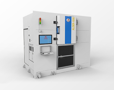
12 inch (compatible with small size) wafer process cavity
Achieving optimal film coverage on high aspect ratio substrates
Modular configurations such as ICP ion source and Loadlock
Depositable thin films: oxides, nitrides, fluorides, metal elements, doped films, laminated films, etc., suitable for various development needs of university research institutes and enterprise R&D departments
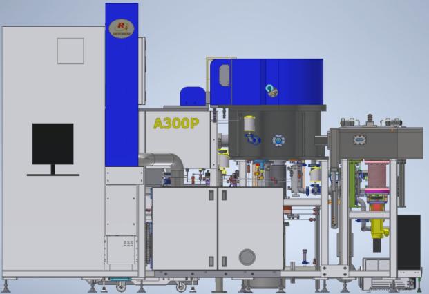
| Deposited film | Oxides, nitrides, fluorides, etc | Wafer size | 300mm | Maximum loading capacity | 1 |
70℃ – 300℃
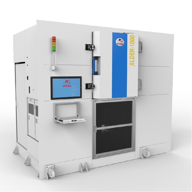
12 inch (compatible with small size) wafer process cavity
Achieving optimal film coverage on high aspect ratio substrates
Modular configurations such as ICP ion source and Loadlock
Depositable thin films: oxides, nitrides, fluorides, metal elements, doped films, laminated films, etc., suitable for various development needs of university research institutes and enterprise R&D departments
High cleanliness wafer and non particle coating scheme can ensure the surface cleanliness of the substrate during the coating process
Loadlock automatic loading and unloading of substrates

Follow official account
Copyright ? 2023 Optorun Semiconductor System Corporation 滬ICP備2023009503號-1